
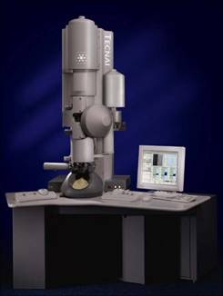
Instrument name: Tecnai G2 F20 U-TWIN Transmission Electron Microscope (Tecnai G2 F20 U-TWIN TEM)
Manufacturer: FEI Company
Specifications:
•Electron source: Schottky field emitter
•Maximum accelerating voltage: 200 kV
•Point resolution: 0.19 nm
•Line resolution: 0.102 nm
•Information limit: 0.12 nm
•STEM HAADF resolution: 0.14 nm
•Magnification range: 25 x - 1,000 kx
•Maximum tilt angle: ±24°
•Minimum energy spread: 0.7 eV or less
•EDX resolution: 136ev
Accessories:
•Gatan GIF Tridiem energy filter
•Gatan 894 CCD camera
•STEM system and HAADF detector
•EDX detector
Functions:
High performance in TEM imaging, STEM imaging and Nano-Analysis, including BF, DF, HRTEM, SAED, STEM-HAADF, EELS, EFTEM, EDX, etc.
It is optimized for complete materials characterization by combining HRTEM with HRSTEM and advanced spectrum imaging in EELS and EDX.
For further information, please contact Dr. QI Xiaoying. Tel: +86-10-82545516, email: qixy@nanoctr.cn
Photo:
 Close Page
- Text Size: A A A
 Printer Friendly