
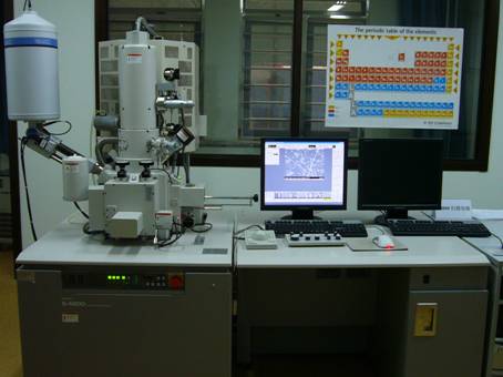
Hitachi S-4800 Scanning Electron Microscope
Hitachi S-3400 Scanning Electron Microscope
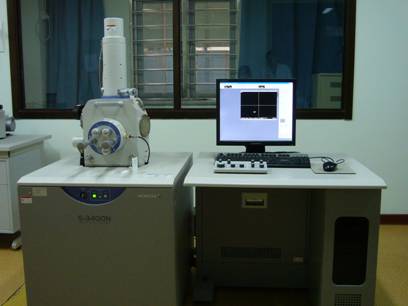
Scanning Electron Microscope (SEM) can be used to observe and analyze the surface morphology of various materials. SEM owns the advantages of high Resolution, deep scope, excellent 3D effect, etc. The resolutions of S-4800 and S-3400 SEM are about 1nm and 3nm, respectively. And its work distance can be changed from 3mm to 30mm. The highest acceleration voltage of S-4800 and S-3400 SEM is 30KV. The obtained information is abundant by using the Images-Analysis of SEM to observe the microstructure. As the requirement of advanced materials increases, the application of SEM testing technology in advanced materials field is more and more important.
The Hitachi S-4800 is a truly versatile platform comprising impressive high resolution performance, advanced detection technology, and a user interface that makes it possible to capture even the most short lived moments accurately and clearly. It employs a semi-in-lens design for large sample accommodation while achieving ultra-high resolution comparable to performance only available with in-lens UHR SEMs.
Hitachi S-4800 Scanning Electron Microscope
Hitachi S-3400 Scanning Electron Microscope
Scanning Electron Microscope (SEM) can be used to observe and analyze the surface morphology of various materials. SEM owns the advantages of high Resolution, deep scope, excellent 3D effect, etc. The resolutions of S-4800 and S-3400 SEM are about 1nm and 3nm, respectively. And its work distance can be changed from 3mm to 30mm. The highest acceleration voltage of S-4800 and S-3400 SEM is 30KV. The obtained information is abundant by using the Images-Analysis of SEM to observe the microstructure. As the requirement of advanced materials increases, the application of SEM testing technology in advanced materials field is more and more important.
The Hitachi S-4800 is a truly versatile platform comprising impressive high resolution performance, advanced detection technology, and a user interface that makes it possible to capture even the most short lived moments accurately and clearly. It employs a semi-in-lens design for large sample accommodation while achieving ultra-high resolution comparable to performance only available with in-lens UHR SEMs.
 Close Page
- Text Size: A A A
 Printer Friendly