
The Tecnai G2 20 S-TWIN TEM is designed to offer an imaging and analysis solution for life sciences, materials sciences, nanotechnology, and the semiconductor and data storage industries. A wide range of functionality and techniques is available and can be combined on the Tecnai G2 20 S-TWIN TEM, to name a few: high contrast imaging, HR-TEM, SAED, CBED, EDX, using embedded detectors and components like BF/DF, CCD and corrected optics.
Manufacturer: FEI Company
Essential specification:
High tension: 200kV
Electron source: LaB6 or W emitter
TEM point resolution: 0.24nm
TEM line resolution: 0.14nm
Minimum focus step: 1.5nm
TEM magnification range: 25×-1030k×
Maximum tilt angle with double-tilt holder: ±40º
Accessories: 1K×1K CCD camera and EDX detector
Energy resolution: 136eV
For further information, please contact Ms. CHANY Huaiqiu. Tel: +86-10-82545519, email: changhq@nanoctr.cn
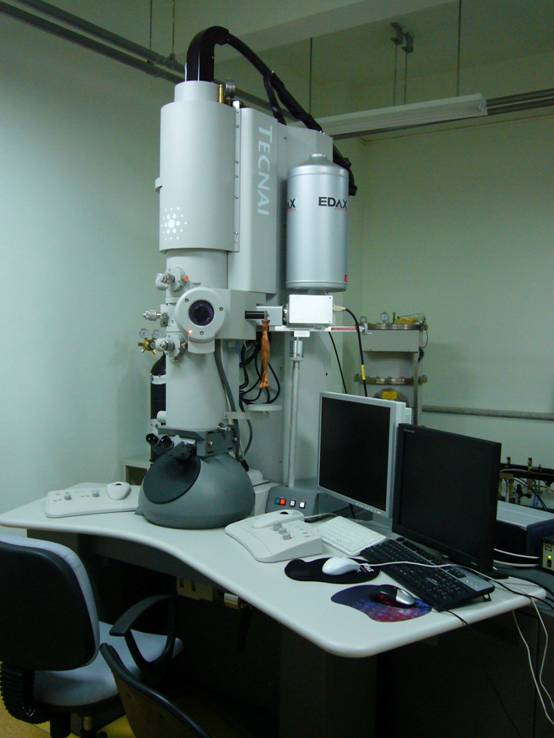
 Close Page
- Text Size: A A A
 Printer Friendly