
The scanning probe microscope is an imaging tool with a vast dynamic range, spanning the realms of optical and electron microscopes. It is also a profiler with unprecedented resolution. The Dimension 3100 scanning probe microscope utilizes standard and advanced SPM imaging modes to measure surface characteristics for semiconductor wafers, lithography masks, magnetic media, CDs/DVDs, biomaterials, optics, and other samples up to 200mm in diameter. Precise laser tracking and the ability to change scanning techniques without tools guarantee flexibility and ease of use. The system's NanoScope 3D controller can scan from the maximum scan size to a few nanometers with full 16-bit resolution on all scan waveforms and on each axis.
For further information, please contact Ms. ZHU Xiaoyang. Tel: +86-10-82545517, email: zhuxy@nanoctr.cn
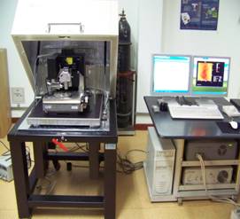
 Close Page
- Text Size: A A A
 Printer Friendly