Two-dimensional (2D) semiconductors, such as transition metal dichalcogenides (TMDs), are considered candidate materials for extending Moore's Law due to their atomic thickness and excellent properties. Achieving precise control over the conductivity type and magnetic properties of 2D semiconductors, through doping is a critical foundation for building functional electronic devices. However, conventional chemical vapor deposition (CVD) methods face challenges in achieving elemental doping across the periodic table.
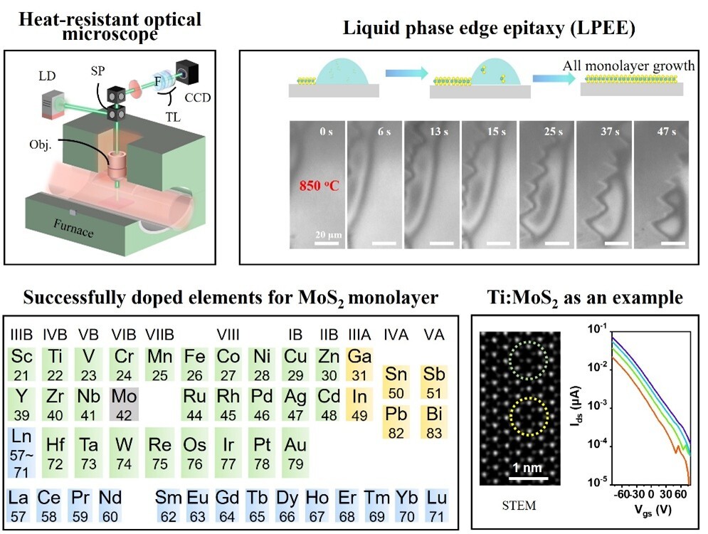
To address this challenge, the "2D semiconductor" research group of NCNST has developed a general doping approach. First, the team developed a high-temperature resistant optical microscope capable of withstanding temperatures up to 950°C. This innovation acts like installing an eye inside the CVD, enabling real-time, in-situ observation of the growth process of MoS2 monolayer. This provided an unprecedented perspective on the crystal growth dynamics (Nano Lett.2024, 24, 5498). Leveraging this unique observational capability, they subsequently developed the Liquid Phase Edge Epitaxy (LPEE) technique for growing TMD monolayer (J. Am. Chem. Soc.2023, 145, 11348). This method laid the foundational approach for intentionally introducing dopant elements during the growth of 2D materials.
In their recently published work on Advanced Materials, the research team successfully incorporated over 40 different elements into MoS2 monolayer using the LPEE technique. The dopants span from transition metals, rare-earth metals, to main group elements. This achievement led to the creation of rarely observed p-type transistors (via Ti, Zn, and Au doping) and soft ferromagnetic semiconductors (via Ce, Nd, Dy, and Ho doping). Furthermore, first-principles calculations revealed a significant correlation between the doping behavior of transition metals in MoS2 and their group in the periodic table: elements from groups IIIB to VIIB tend to substitute at Mo sites, groups IB and IIB elements are prone to form adatom configurations on the lattice surface, while group VIII elements exhibit more diverse doping configurations. This work provides a solid material foundation for the future construction of all-MoS₂ integrated circuits—directly integrating p-type, n-type, metallic interconnects, and even magnetic components—through selective doping.
This collaborative work was completed by the NCNST-OU Collaborative Laboratory, the University of Science and Technology Beijing (USTB), and other institutions. The co-first authors include Zunaira Urooj (a Pakistani student at NCNST), Junxu Mao from NCNST, You Li from USTB, and Haiming Sun from Osaka University. Corresponding authors include Prof. TAN Ting and Prof. XIE Liming from NCNST, Prof. QI Junjie from USTB, and Prof. Kazutomo Suenaga from Osaka University, Japan.

