To address this issue, Prof. LIU Xinfeng from the National Center for Nanoscience and Technology, China (NCNST), in collaboration with Prof. XU Haiyang's team from Northeast Normal University, published a research paper titled "Defect-Engineered Reduction of the Carrier Multiplication Threshold in Monolayer WS2 to 1.6Eg" in ACS Nano. The study breaks the carrier multiplication limit of TMDs to 1.6Eg through defect engineering. By introducing in-gap states (IGS) to enhance electron-phonon coupling (EPC), the second electron can transition into the conduction band through IGS-assisted upconversion after absorbing energy, thereby realizing a low-threshold energy CM (LTE-CM) process at a photon energy of 1.6Eg. The research utilized chemical vapor deposition (CVD)-grown monolayer WS2 and introduced high-density symmetric disulfur vacancies (V2S) through thermal annealing. The types and concentrations of defects were confirmed by techniques such as scanning transmission electron microscopy (STEM) and X-ray photoelectron spectroscopy (XPS), revealing that symmetric V2S is the most effective in promoting LTE-CM.
This study demonstrates an ultra-low threshold carrier multiplication process in monolayer WS2 enabled by artificially engineered in-gap states and strong electron-phonon coupling. Optoelectronic measurements show that when the photon energy exceeds 1.6Eg, the photoresponsivity (R) and internal quantum efficiency (IQE) of the device increase sharply, and the power-dependent exponent of the photocurrent exceeds 1, indicating obvious CM characteristics. Transient absorption (TA) spectroscopy further verifies the occurrence of CM, showing that when the pump photon energy exceeds 1.6Eg, the carrier quantum yield (QY) increases from 1 to nearly 2, indicating that each photon generates more than one electron-hole pair. This is the first experimental discovery of a carrier multiplication process with a threshold energy below 2Eg. Temperature-dependent experiments and Raman spectra confirm that V2S significantly enhances EPC and promotes the phonon-assisted upconversion process. Density functional theory (DFT) and ab initio molecular dynamics (AIMD) simulations reveal the key role of in-gap states in the CM process: the introduction of V2S forms intermediate energy levels in the bandgap. Valence band electrons excited by impact ionization first transition to the intermediate states, and then jump to the conduction band through the degeneracy and lifting of degeneracy processes of the intermediate energy levels and the multiphonon-assisted upconversion process, completing the LTE-CM process. Theoretical calculations provide the energy required for each transition process, revealing that lattice softening caused by symmetric V2S is most conducive to the aforementioned processes, which is consistent with the experimental results.
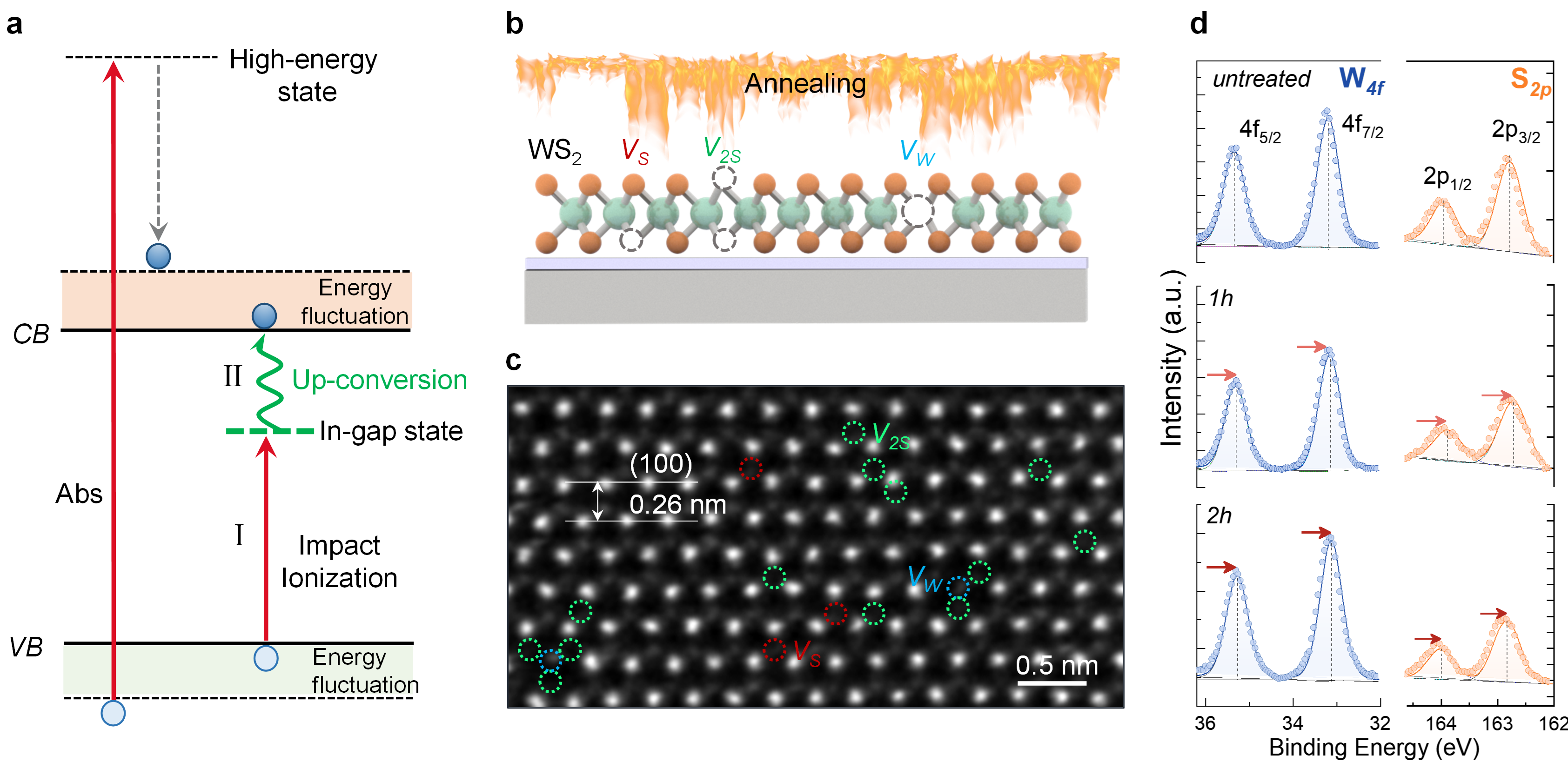
Figure 1. Design of LTE-CM in monolayer WS2. (a) Schematic diagram of the LTE-CM process. (b) Schematic of annealing for vacancy-doped WS2, indicating three types of vacancies: monosulfur vacancy (VS), symmetric disulfur vacancy (V2S), and tungsten vacancy (VW). (c) Atomically resolved STEM image of WS2 annealed for 2 hours, with three defect types marked by dashed circles of corresponding colors. (d) XPS spectra of W 4f/5p and S 2p core levels of untreated WS2 and samples annealed for 1 hour and 2 hours. Red arrows indicate the redshift of the spectral peaks with increasing annealing time.
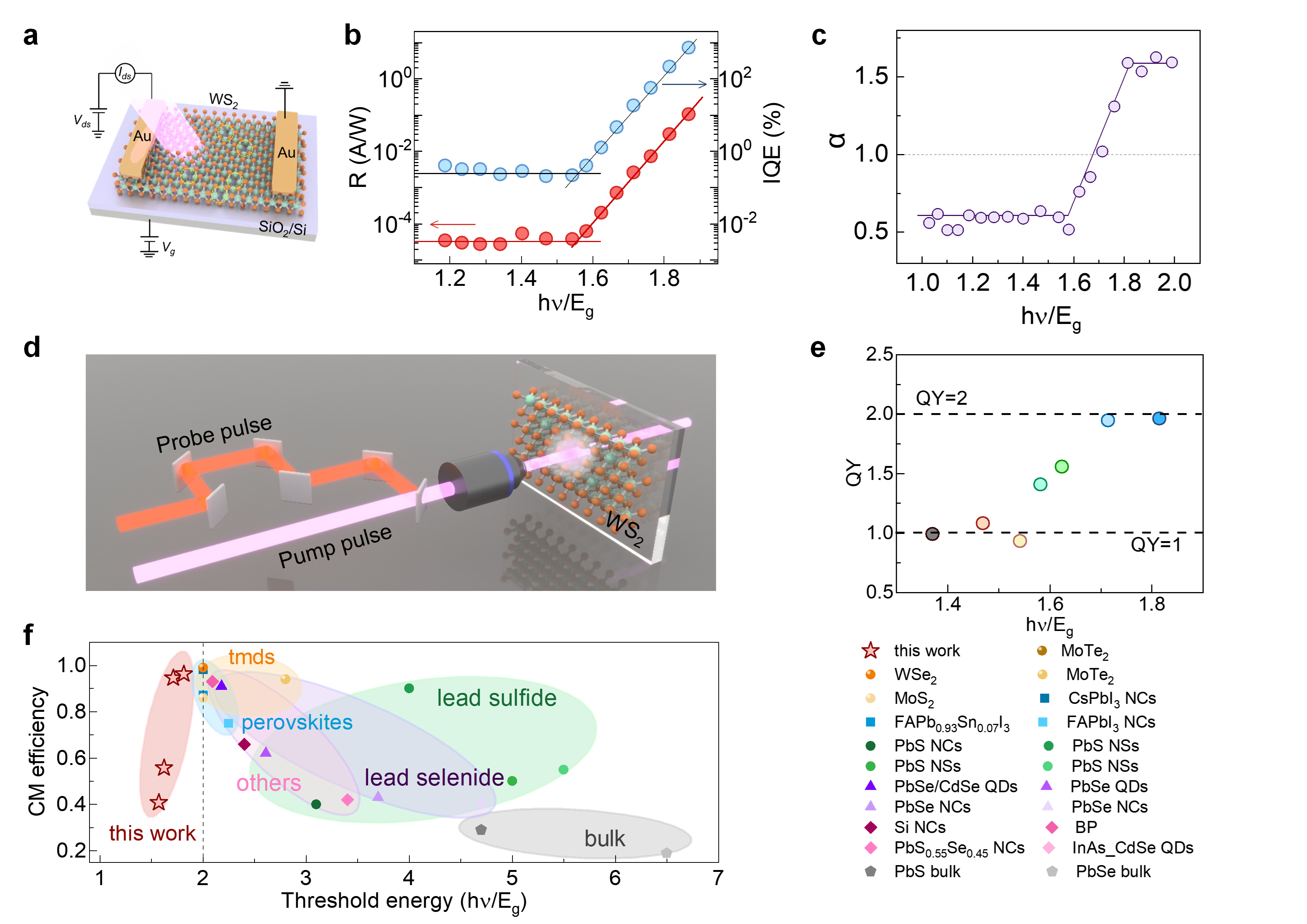
Figure 2. Experimental evidence of LTE-CM. (a) Schematic diagram of a monolayer WS2 device on a Si/SiO2 substrate. (b) Responsivity (R) and internal quantum efficiency (IQE) under different excitation photon energies. (c) Summary of the α parameter under different photon energies. (d) Schematic diagram of the TA setup. (e) Dependence of QY on pump photon energy. (f) Comparison of CM behavior between monolayer WS2 and other materials.
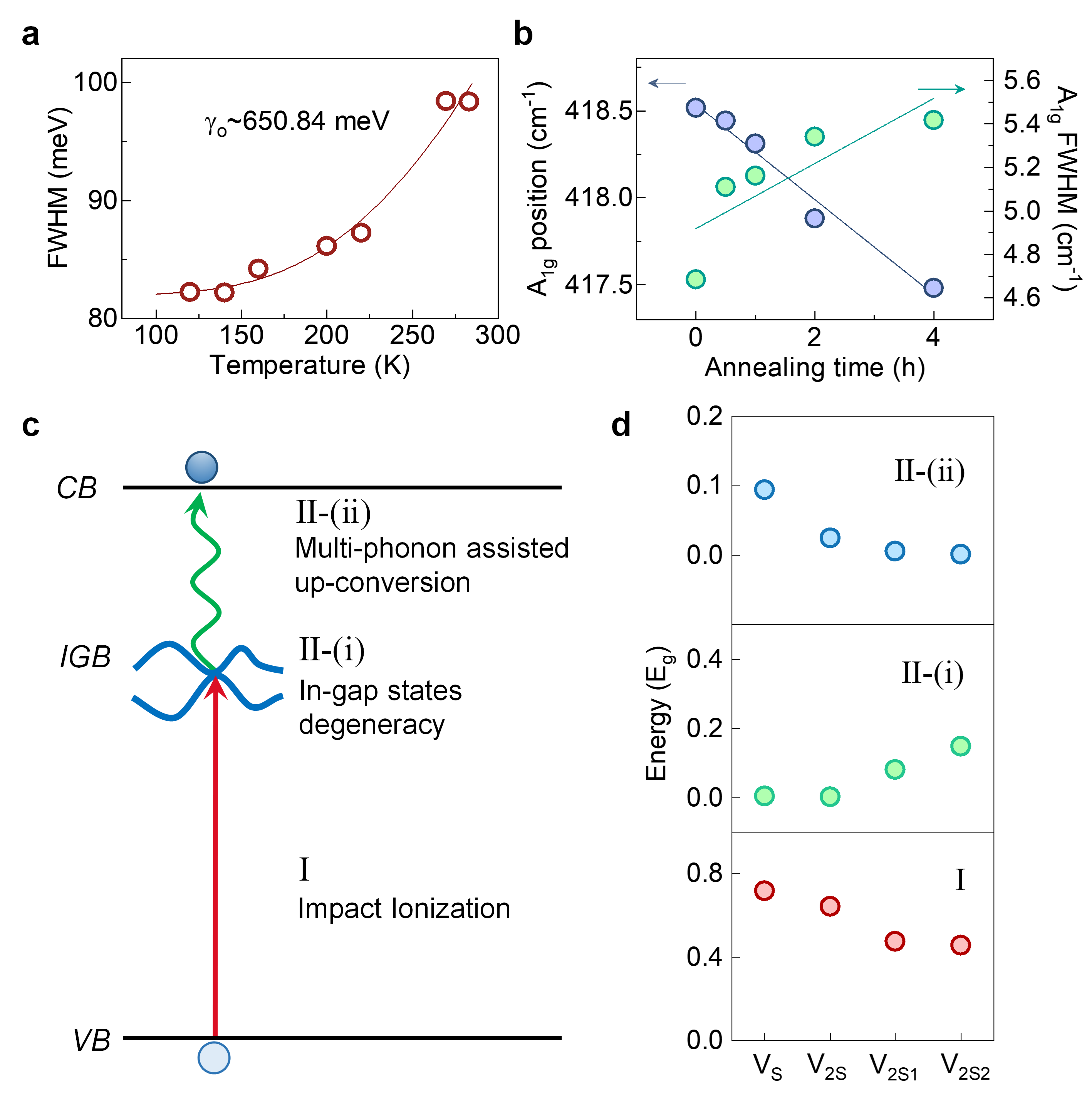
Figure 3. Mechanistic explanation of LTE-CM. (a) Temperature dependence of the full width at half maximum (FWHM) of the A exciton in V2S-WS2 excited by a 320 nm laser. Solid lines are fitting curves using the Debye-Einstein approximation. (b) Variations of the peak position and FWHM of the out-of-plane phonon mode of V2S-WS2 with annealing time, excited by a 488 nm laser. (c) Schematic diagram of the dynamics of the second electron in LTE-CM. (d) Statistics of the energies required for the three processes in four different WS2 configurations.
Contact:
LIU Xinfeng
National Center for Nanoscience and Technology (NCNST)
E-mail: liuxf@nanoctr.cn

