Recently published in Nature Synthesis, a research team led by Prof WANG Zhenxing from the National Center for Nanoscience and Technology, China (NCNST), has made a significant breakthrough in the controllable preparation of low-dimensional semiconductor thin films. The team established the controllable synthesis of wafer-scale, uniaxially oriented tellurium nanowire films via molecular beam epitaxy based on the substrate molecular engineering.
Tellurium (Te) is a semiconductor material with a one-dimensional chain-like van der Waals structure. It features a bandgap of approximately 0.3 eV, a high hole mobility of up to 1370 cm2·V-1·s-1. It possesses unique properties such as a chiral crystal structure and Weyl bands, showing broad application prospects in high-performance p-type transistors, polarized optics, and spintronics. However, traditional methods like hydrothermal synthesis and chemical vapor deposition often produce materials suffering from poor crystallinity, low ordering, and difficulties in precise control over thickness and morphology.
Addressing these challenges, the research team proposed a novel strategy based on molecular-assisted nucleation. This method utilizes m-plane sapphire substrates, which form parallel-aligned V-shaped groove structures after high-temperature annealing. The surface is then modified with organic molecules possessing an "anchor-rope" structure, such as alkyl imidazoline or oleylamine. One end of these molecules features an "anchor" group (e.g., imidazole, carbon-carbon double bond, amino group) with strong affinity for tellurium atoms, while the other end consists of a long alkyl "rope" chain (containing C-C single bonds) that repels tellurium atoms. After self-assembly within the V-shaped grooves, these molecules create a periodic adsorption potential field for tellurium atoms, guiding their preferential adsorption at the groove bottoms and subsequent oriented growth along the groove direction, ultimately forming highly ordered tellurium nanowire films.
Using this method, the team successfully prepared highly oriented tellurium nanowire films with a size up to 1.3 inches. Remarkably, 99.7% of the nanowires exhibited an orientation angle deviation of less than 5°, and the film thickness could be precisely controlled from 10 nm to several hundred nanometers. Field-effect transistors fabricated based on these films demonstrated excellent p-type electrical performance: among 247 tested devices, the maximum room-temperature hole field-effect mobility reached 560 cm2·V-1·s-1, with an average mobility of 273 cm2·V-1·s-1, and a maximum on/off ratio of up to 104.
This research lays a solid foundation for the application of tellurium-based nanostructures in next-generation electronic devices and provides new insights for the controllable synthesis of other low-dimensional semiconductor materials.
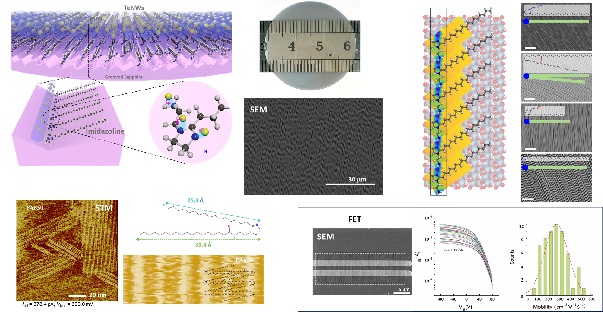
Schematic diagram for the preparation of wafer-scale parallel-aligned Te nanowire films (Image by WANG Zhenxing et al)
Contact: WANG Zhenxing
National Center for Nanoscience and Technology (NCNST)
E-mail: zxwang@nanoctr.cn

