Micro/nanolasers serve as core components of photonic chips, holding significant application promise in high-speed optical communications, high-resolution bioimaging, and sensing. However, their performance typically declines as the laser cavity size decreases due to increased losses within the microcavity and the material itself. This has led to the widely accepted trade-off between smaller size and lower threshold. Overcoming this fundamental limit requires new material systems or cavity designs that deviate from classical scaling laws.
Perovskites have attracted considerable attention due to their structural tunability, facile synthesis, long carrier diffusion lengths, and high luminescence quantum yield. In particular, the high optical absorption coefficient and differential gain make them particularly suitable for low threshold nanolasers. Among them, two-dimensional (2D) and quasi-2D perovskites feature a naturally formed multiple quantum well structure. This induces a strong quantum confinement effect, enabling stable exciton existence at room temperature and favoring the formation of biexcitons. The pronounced Stokes shift of biexcitons will suppress reabsorption losses, which is beneficial for integrated nanoscale light sources.
Recently, a research team led by Prof. LIU Xinfeng from the National Center for Nanoscience and Technology (NCNST) of the Chinese Academy of Sciences (CAS) achieved a critical breakthrough in quasi-2D perovskite microcavities. They achieve a low-threshold (<14 μJ/cm2), ultrafast switchable (~5 ps) biexciton lasing via anomalous scaling effect. By balancing the influences of Auger recombination and exciton binding energy, the team employed an anti-solvent method to fabricate high-quality, phase-pure n=2 Ruddlesden-Popper perovskite microplatelets. Utilizing the naturally formed whispering-gallery-mode optical microcavities within these microplatelets, they systematically investigated the impact of size on lasing performance.
The results revealed that the lasing threshold decreases significantly as the microplatelet size is reduced. This trend is completely opposite to the behavior observed in conventional III-V semiconductors and 3D perovskites. Through combined electric field simulations and spectroscopic analysis, the emission was confirmed to originate from biexciton lasing. They attributed this anomalous scaling to differences in exciton reabsorption processes dependent on cavity size. In smaller microcavities, the photon recycling process is suppressed, allowing biexciton formation and gain to dominate, thereby enabling lower-threshold lasing.
Furthermore, the study found that the biexciton lasing exhibits picosecond-scale optical switching capability. Using a dual-beam excitation, controllable 'shutdown' and 'restart' of the biexciton lasing was achieved. The shutdown time shortens with decreasing cavity size, reaching a minimum of ~5 ps. This indicates that the system not only breaks the conventional performance limits in steady-state operation but also shows significant potential for high-speed optical switching, paving a new path for future applications in ultrafast optical computing and high-speed on-chip optical interconnects.
This work not only reveals a new size-performance mechanism based on the biexciton process but also provides a practical strategy for developing novel nanolasers with low threshold, high speed, and integrability. It holds substantial importance for advancing integrated photonics and compact optical information processing systems. The related research findings have been published in ACS Nano under the title "Anomalous Scaling Enables Lower-Threshold and Ultrafast Switchable Nanolasing in a Phase-Pure Quasi-2D Perovskite Cavity".
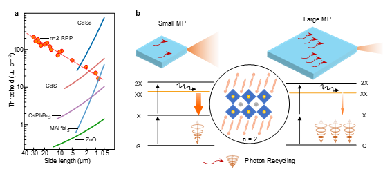
Figure. Quasi-2D perovskite nanolaser with anomalous size-threshold dependence. (a) The lasing threshold decreases with reduced size, opposite to the trend in conventional semiconductors and 3D perovskites. (b) Schematic illustrating the anomalous size dependence arising from the competition between photon recycling and biexciton lasing. (Image by LIU Xinfeng et al)
Contact:
LIU Xinfeng
National Center for Nanoscience and Technology (NCNST)
E-mail: liuxf@nanoctr.cn

