Recently, a research team led by Prof. WANG Zhenxing from the National Center for Nanoscience and Technology (NCNST) has made a significant breakthrough in the field of two-dimensional (2D) semiconductor contact. They proposed a new contact strategy for 2D p-type field-effect transistors based on van der Waals-induced metallic tellurium (m-Te), providing a new direction for the development of 2D logic circuits. The related results were published in Nature Communications.
As the manufacturing process of integrated circuits (ICs) approaches its physical limits, traditional size miniaturization technologies are facing severe challenges. The International Roadmap for Devices and Systems (IRDS) points out that as the 1-nanometer process node technology approaches, there is an urgent need to develop technical routes for new materials and new devices. 2D semiconductor materials have become important candidate materials for breaking through the bottlenecks of advanced manufacturing processes due to their ultra-thin thickness, atomically sharp surface, adjustable band gap, wide variety, and compatibility with silicon-based processes.
However, the practical application of 2D semiconductors still faces multiple obstacles, among which the most notable one is the contact resistance issue. The traditional ion implantation scheme for heavily doping reduces the contact resistance from the perspective of reducing the depletion region width and improving the tunneling injection efficiency, but there is still a lack of non-destructive doping strategies suitable for 2D semiconductors at present. In addition, the metal-induced bandgap states at the contact interface and the intrinsic defect states of the material can cause the Fermi level to be pinned within the bandgap, forming a high charge injection barrier. It is difficult to achieve ohmic contact merely by matching the metal work function. Although previous studies have made progress in n-type semiconductor contacts through methods such as semi-metal contacts and atom-layer bonding, high-performance and highly compatible contact schemes for p-type two-dimensional field-effect transistors still urgently need to be broken through.
The team's research found that the metallic tellurium (m-Te) with a monoclinic P21 structure can grow in an oriented manner under the lattice-induced effect of molybdenum disulfide (MoTe2). When it is used as the p-type electrical contact material for MoTe2 2D field-effect transistors, the p-type contact resistance is as low as 1.6 kΩ μm, which can be attributed to the matching band edge, weak metal-induced states and atomically sharp contact interfaces.
At a channel length of 130 nm, the device's on-state current density is as high as 124 μA μm-1, and the maximum on/off ratio is 107. Its comprehensive performance ranks among the top of the reported p-type 2D field-effect transistors. This work provides a new direction for the in-situ growth of metal phase chalcogenide elements for optimizing the contact of 2D transition metal chalcogenide transistors.
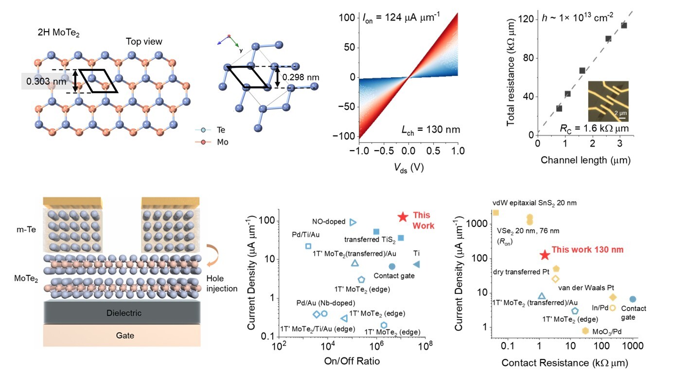
Figure. Two-dimensional MoTe2 field-effect transistor p-type contact based on metallic tellurium (Image by ZHU Yuhan et al)
Contact: WANG Zhenxing, WANG Feng
National Center for Nanoscience and Technology (NCNST)
E-mail: wangzx@nanoctr.cn, wangf@nanoctr.cn.

