Recently, a research team led by Prof. LIU Xinfeng from the National Center for Nanoscience and Technology (NCNST) of the Chinese Academy of Sciences (CAS) reported the giant out-of-plane exciton emission enhancement in InSe via plasmonic nanocavity with 34000 of enhancement factor. The research is published on Nano Letters. (DOI: 10.1021/acs.nanolett.2c04902)
The out-of-plane (OP) exciton, which is also called “dark excitons”, shows a dipole moment perpendicular to the atomic plane. The superior properties of OP exciton, such as p-polarized emission, supporting higher bias fields and steerable spin-valley coupling, determine it is attractive participant for novel photonic applications, for instance, the generation of radially polarized sources, integrated photonic devices and quantum communications. As the medium for the light-matter interaction in two-dimensional semiconductor materials, unlike the in-plane (IP) excitons, which dominate the response to a perturbative optical field, the OP excitons are barely involved since their absorption is prohibited by the selection rule. The forbidden transition of OP excitons to normally incident light hinders exciton-photon interactions to weaken their optical response.
At present, the optical performance regulation of IP exciton in two-dimensional semiconductor materials has been widely studied, but effective optical performance regulation of OP exciton still lacks a complete understanding, especially how OP exciton couples with the normally incident light, stimulating effective light-matter interaction. Solving the problem is very important to optimize and expand the application of OP exciton-based semiconductor materials. First and most significantly, the proper structural design and sample selection are essential.
“InSe is a two-dimensional semiconductor material with OP excitons. Can we combine InSe with a plasmonic nanocavity to study the regulation optical properties of OP excitons?” said LIU Xinfeng from NCNST, one of the paper’s corresponding authors.
In this work, the researchers mechanically exfoliated an InSe flake from a bulk InSe crystal and transferred it to an Au-SiO2/Si substrate using site-specific transfer. Next, silver cubes were monodispersed on the transferred InSe to construct the InSe-embedded plasmonic nanocavity system. ?They successfully constructed the sample structure using a combination of microscopic imaging and SEM, with only one silver cube on the InSe surface to exclude the influence of other silver cubes.
The researchers have demonstrated that the plasmonic nanocavity can generate OP localized electric fields under normal incident light, and the exciton-plasmon interaction can be efficiently realized using the finite-difference time-domain simulation.
The researchers reveal the inverse relationship between the PL enhancement factor and InSe thickness, and the local electric field intensity increased with the decrease of InSe thickness, and prove that the resonance-excited plasmonic nanocavity mode obtains the optimal enhancement factor of 34000, which is verified in the normalized scattering and reflection spectra. Due to the change of local state density, the radiation rate of OP excitons is accelerated by Purcell effect. The researchers successfully reproduce the experimental data by combining the simulation of OP local electric field and Purcell factor.
In order to identify the exciton species and their radiation patterns. The researchers measured the k-space imaging and calculated the contribution ratio of OP excitons. They prove that the signal mainly comes from OP excitons, and the contribution of IP excitons is negligible. The extracted angle-resolved PL spectra confirmed the enhanced emission directionality of OP excitons results from the plasmonic nanocavity.
LIU said this study expands the understanding of the optical property regulation of OP excitons from the perspective of space, time and energy, and provides a way for the design and performance optimization of OP dipole-oriented photonic devices on chip.

Figure1. (a) Schematic of an InSe-encapsulated plasmonic nanocavity. The inset shows a cross-sectional schematic of the system. (b) PL enhancement factor of InSe as a function of the excitation wavelengths. The inset is a schematic of the transient reflection measurement. (Image by LIU Xinfeng et al)
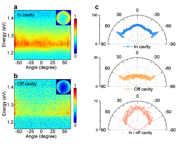
Figure2. (a) Angle-resolved emission spectrum of InSe in cavity. (b) Angle-resolved emission spectrum of InSe off cavity. (c) Angle-resolved PL spectra of the InSe at different positions. (Image by LIU Xinfeng et al)
Contact:
LIU Xinfeng
National Center for Nanoscience and Technology

