Recently, a research team led by Prof. LIU Xinfeng from the National Center for Nanoscience and Technology (NCNST) of the Chinese Academy of Sciences (CAS) reported the exciton emission enhancement in monolayer WS2 on a silicon substrate via a Fabry–Pérot microcavity with 438 of enhancement factor. The research is published on Nano Letters and is published online in Supplementary Cover form.
Two-dimensional monolayer transition-metal dichalcogenides (TMDs) are direct band gap semiconductor materials, which break through the thickness limit of bulk materials, and the reduction of Coulomb screening effects produces large exciton binding energy, ensuring their exciton emission intensity at room temperature. The nonbonding surface of monolayer TMDs facilitates their transfer or direct growth onto diverse substrates, eliminating concerns related to lattice mismatches. However, low quantum yield and short photoluminescence (PL) lifetime are the main factors restricting the practical application of monolayer TMDs materials. Due to the atomic thickness of monolayer TMDs, the light-matter interaction is limited, resulting in weak exciton absorption and emission. In addition, the substrate on which monolayer TMDs grows and transfers has significant influence on its exciton PL yield. This impact is primarily due to substrate-induced doping monolayers and the defect-related nonradiative recombination processes.
Therefore, it is still a difficult task to realize the ideal monolayer TMDs exciton emitter at room temperature. Orbital angular momentum, gate voltage and surface engineering methods have been used to enhance the exciton effect of monolayer TMDs. However, the PL enhancement of existing monolayer TMDs materials in silicon-based microhole systems is only one order of magnitude, and there is a lack of comprehensive and detailed explanation of the mechanism of PL enhancement, which is very important for the application and development of silicon-based monolayer TMDs materials in miniaturized optoelectronic devices.
The researchers used inductively coupled plasma etching method to prepare SiO2/Si substrate microhole array, and obtained monolayer WS2 by mechanical exfoliation and transferred to microholes on SiO2/Si substrate to construct Fabry-Perot microcavity. The optical imaging, scanning electron microscopy, and atomic force microscopy were used to characterize the sample structure. The PL enhancement of monolayer WS2 in the Fabry-Perot cavity was demonstrated by steady-state PL spectra and PL imaging.
The researchers obtained the largest exciton PL enhancement factor ~438 in monolayer WS2 by regulating the detuning between the excitation wavelength and the Fabry-Perot cavity mode. The temperature-dependent PL spectra show that the collected signal is mainly from exciton emission at room temperature, and due to the weakening of the substrate effect, multiple exciton emission occurs in monolayer WS2 on cavity at low temperature, which reflects better sample quality.
The researchers demonstrated that suspended monolayer WS2 weakens the substrate effect, reduces the generation of trions, and causes more excitons to decay in the form of radiation recombination, resulting in a longer exciton radiation lifetime by using time-resolved PL spectra and transient absorption spectra.
This study proves that the coupling system of monolayer TMDs and silicon-based microholes is a practical platform for enhancing exciton emission and weakening substrate effect, which opens a way for the development of monolayer TMDs materials in the field of integrated optoelectronics.
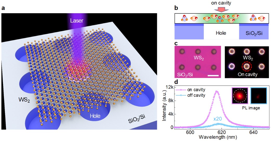
Figure 1. (a) Schematic of the monolayer WS2 sitting on a hole patterned SiO2/Si substrate. (b) A cross-sectional schematic of the monolayer WS2 sitting on top of the SiO2/Si substrate with micron-scale holes. (c) Optical bright and dark field images of monolayer WS2 on cavity. The scale bar is 10 μm. (d) PL spectrum of monolayer WS2 on cavity and off cavity. Inset: PL images of monolayer WS2 on cavity and off cavity at the same excitation conditions. (Image by LIU Xinfeng et al)
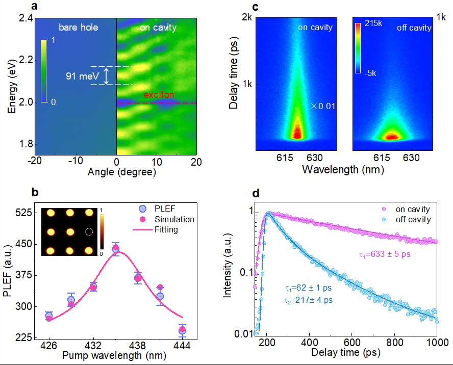
Figure 2. (a) Normalized angle-resolved reflectance spectra of the bare hole (without monolayer WS2) and the monolayer WS2 on cavity. (b) The PLEF of monolayer WS2 as a function of the excitation wavelengths. The illustration shows the PL mapping for monolayer WS2 on cavity. (c) The TRPL spectra of monolayer WS2 on cavity and off cavity. (d) The PL decay dynamics of monolayer WS2 on cavity and off cavity. (Image by LIU Xinfeng et al)
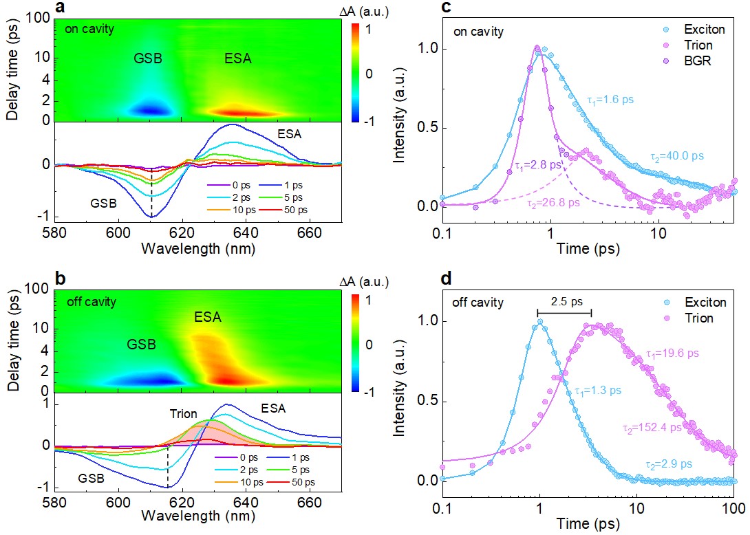
Figure 3. (a, b) TA mapping (top panel) and TA spectra (bottom panel) of monolayer WS2 on cavity and off cavity. (c, d) Decay dynamics of monolayer WS2 on cavity and off cavity. (Image by LIU Xinfeng et al)
Contact:
LIU Xinfeng
National Center for Nanoscience and Technology (NCNST)
E-mail: liuxf@nanoctr.cn

